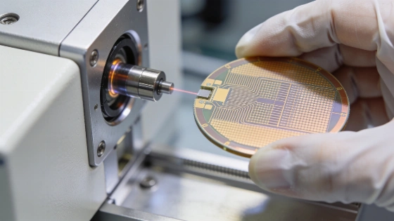
NLM Photonics, LIGENTEC SA and Spark Photonics have fabricated silicon nitride organic-hybrid modulators that could connect low-loss visible photonics with quantum routing and laser control.
NLM Photonics, LIGENTEC SA and Spark Photonics have fabricated what the companies describe as the first Silicon Nitride Organic Hybrid modulators on a commercial photonics platform. The result is a proof of concept rather than a demonstrated quantum system, but it addresses a practical weakness in integrated photonics: standard silicon circuits absorb visible light, while silicon nitride can guide it across a much broader wavelength range.
The work is best understood as a materials-and-fabrication milestone. It combines LIGENTEC's passive silicon-nitride platform with NLM's organic electro-optic materials and is aimed at active photonics beyond conventional telecom bands. The approach could eventually support visible quantum photonics, quantum-key-distribution hardware and laser-control functions, but the supplied reports do not establish a complete quantum processor, network or trapped-atom experiment.
Silicon photonics is highly developed for telecom wavelengths, yet material absorption in the visible spectrum limits where active silicon circuits can operate. Silicon nitride offers low propagation loss and a broad transparency window. NLM materials describe Selerion(TM) organic electro-optic glass as transparent from the visible range to 2.5 µm, a span relevant to optical transitions that fall outside conventional telecom bands. Recent work on visible-band SiN photonic integrated circuits further illustrates why the material is being considered for this part of the spectrum in visible-band SiN research.
That wavelength coverage matters for photonic-qubit routing, quantum key distribution and laser control in trapped-atom systems. In each case, the useful optical transition may lie in the visible or near-infrared range rather than around the wavelengths most common in datacom. The underlying principle is established photonics rather than a new quantum effect: SiN provides passive guidance, while the organic layer is intended to provide an electrically controlled change in optical phase or intensity.
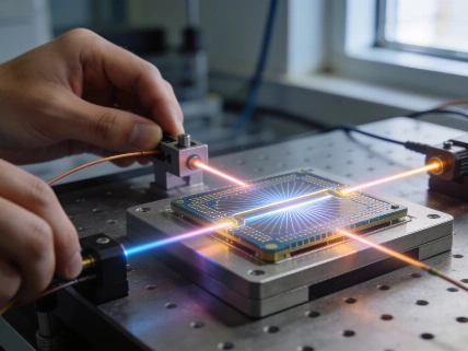
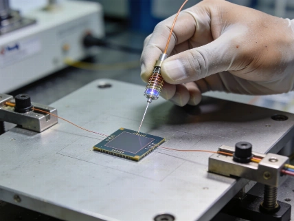
The new devices combine the passive SiN waveguide platform with Selerion(TM) organic electro-optic glass. NLM Photonics supplies the OEO material and poling process, LIGENTEC provides foundry fabrication on its commercial low-loss SiN wafer platform, and Spark Photonics developed the layout and process-design rules needed to place the active material and electrical structures on top of the finished photonic substrate.
The manufacturing strategy is important because it does not require the organic electro-optic material to survive every step used to build the underlying silicon-nitride circuit. Instead, NLM's Selerion(TM) layer, metallization and poling are applied as back-end-of-line processing steps. This separates the thermal and chemical demands of passive waveguide fabrication from the later formation of the active modulator and reduces the temperature constraints imposed on the organic material during construction of the base circuit.
An electro-optic modulator changes the intensity or phase of light in response to an electrical signal. In this case, the organic material is intended to provide the electrically controlled optical response while the SiN substrate supplies low-loss guidance. The reported demonstration establishes fabrication and integration on the platform; the supplied material does not report modulation speed, optical loss, modulation depth, drive voltage or device yield.
Those missing quantities define the next scientific test. A credible device comparison would need measurements across multiple devices and wafers, including insertion loss, electro-optic bandwidth, switching energy, thermal stability, optical damage thresholds and process variation. A future peer-reviewed report in a journal such as Nature would also need to distinguish single-device performance from statistically representative manufacturing data.
The proposed uses are technically specific but remain applications for future device and system testing. A modulator could help route photonic qubits through an integrated circuit or control optical signals used in quantum key distribution. In trapped-atom experiments, it could contribute to laser control. None of those applications is shown here as a complete operating quantum processor, quantum network or atom-control platform.
That distinction is central. The announcement provides no qubit count, measured gate or readout fidelity, coherence time or quantum key rate. It also provides no comparison with a classical optical-control system and no evidence of independent replication. The appropriate reading is therefore a materials and fabrication milestone: a route has been demonstrated for combining active organic electro-optic functionality with passive SiN photonics across visible and near-infrared wavelengths.
The broader quantum-hardware field faces the same division between a promising component and a useful system. For readers following how quantum technologies move from software and algorithms toward physical infrastructure, an earlier education report illustrates the contrasting software and workforce side of that pipeline. This device work addresses the optical layer instead. The eventual engineering questions resemble those encountered in other precision platforms developed at institutions such as MIT and CERN: whether laboratory functionality remains stable when integrated into a larger, calibrated and repeatable system.
NLM's technical milestone arrives alongside an expansion of its investor base intended to support materials supply and a multi-foundry manufacturing pipeline. Pangaea Ventures and Diamond Edge Ventures joined the company's investors, with Diamond Edge Ventures serving as Mitsubishi Chemical Corporation's venture arm. Emerald Technology Ventures, Tokyo Ohka Kogyo, Idemitsu Kosan, Oregon Venture Fund and StoryHouse Ventures provided follow-on investments. Optica's corporate news coverage also reports the expansion of NLM's investor base with Pangaea Ventures and Diamond Edge Ventures.
The strategic value claimed for that syndicate is practical rather than merely financial. Industrial chemical supply, wafer processing and packaging support become increasingly important when an organic-hybrid device must move from a single-wafer demonstration toward repeated foundry production. Yet investment does not establish manufacturing yield or long-term reliability. Those questions require data across devices and wafers together with measurements of optical loss, electrical drive performance, thermal stability and process variation.
Silicon nitride offers the optical window for applications that silicon cannot serve efficiently in the visible range, while Selerion(TM) supplies the active electro-optic layer that passive SiN lacks. Lewis Johnson, NLM Photonics' co-founder and chief technology officer, characterized the collaboration as a milestone for commercial NOH photonic integrated circuits; the companies also plan further optimization toward more compact and efficient active SiN devices. The significance lies in joining a commercial foundry process to a material system aimed at visible and near-infrared control. The next test is whether the devices deliver repeatable performance under the loss, noise, packaging and calibration constraints of real photonic systems.
In an organic-hybrid modulator, the electrical signal does not become a qubit by itself. It changes an optical property of the material so that a guided light field can be varied in phase or intensity. For quantum photonics, that control must eventually be measured against photon loss, stability and noise because a component that works on a wafer is not automatically a reliable qubit router or secure-communication device. As with other advanced photonic systems studied across the research community, including work reported through NASA and leading optics journals, the decisive evidence will be quantitative system-level performance rather than the existence of an integration route alone.