PsiQuantum has finalized a $100 million CHIPS Act award with the US Department of Commerce to accelerate domestic manufacturing of photonic quantum computing components and strengthen the onshore supply chain for advanced quantum hardware
In a decisive move for US quantum hardware infrastructure, PsiQuantum has executed a $100 million research and development award under the CHIPS and Science Act, formalizing a partnership with the US Department of Commerce to expand domestic manufacturing of photonic quantum computing components. This direct federal investment is designed to address persistent bottlenecks in wafer-scale fabrication and supply chain security for quantum devices built on photonic architectures.
Wafer-Scale Photonic Fabrication
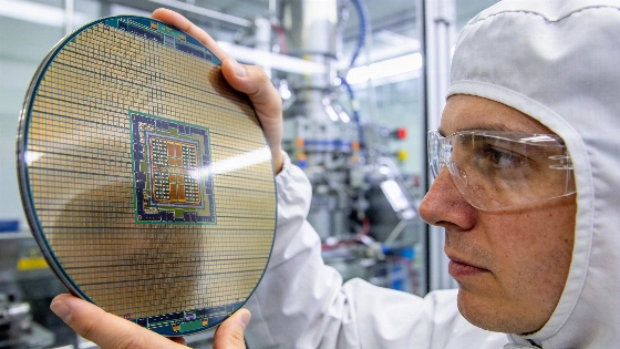
The agreement channels capital into PsiQuantum's Santa Clara facility, where the company aims to accelerate 300-millimeter wafer production of barium titanate (BTO) thin films. BTO is a high-performance electro-optic material critical for low-loss optical switches, a core element in photonic quantum circuits. The process relies on molecular beam epitaxy (MBE) tools to deposit and control the thin-film layers with atomic precision, a requirement for reproducible device performance at scale. PsiQuantum's roadmap includes scaling up BTO wafer throughput and integrating these materials into photonic chips for quantum logic and routing.
Component Yield and System Integration
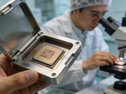
Beyond material growth, the CHIPS Act funding supports performance optimization and yield improvement for high-temperature single-photon detectors, as well as automated chip-to-fiber packaging lines at PsiQuantum's Milpitas assembly site. These steps are essential for moving from laboratory prototypes to manufacturable quantum hardware, where device yield, packaging reliability, and detector efficiency directly constrain system-level performance. The company's manufacturing pipeline has already involved approximately $200 million in US supplier spending in 2025, and the new award is intended to reinforce domestic supply chains for critical quantum components.
Foundry Partnerships and Defense Links
PsiQuantum's photonic chips, branded as "Omega" chipsets, are fabricated in partnership with GlobalFoundries using standard 300-millimeter silicon photonics lines in Malta, New York. This foundry integration is a key test of whether advanced quantum photonic devices can be produced using established semiconductor infrastructure. In parallel, PsiQuantum maintains defense research collaborations, including photonic circuit integration with the Air Force Research Laboratory and a $125 million expansion under DARPA's Quantum Benchmarking Initiative. For context on alternative quantum hardware integration, see our reported earlier coverage of trapped-ion quantum processors linked to supercomputing clusters.
Engineering and Scalability Challenges
While the CHIPS Act award marks a significant policy and funding milestone, the technical path to scalable, fault-tolerant photonic quantum computing remains complex. Achieving high-yield, low-loss photonic devices at wafer scale requires not only precise material deposition but also tight control over fabrication variability, optical coupling, and detector integration. Automated packaging and system-level assembly introduce further engineering hurdles, especially as device counts and circuit complexity increase. The company's reliance on established foundry processes offers a plausible route to scale, but reproducibility, error rates, and integration with quantum error correction protocols will ultimately determine whether these investments translate into practical quantum advantage.
Physical qubits in photonic quantum computing are typically encoded in single photons, with quantum information carried by properties such as polarization or path. Unlike superconducting or trapped-ion systems, photonic qubits are less susceptible to certain types of decoherence but face unique challenges in loss, detection efficiency, and circuit integration. Achieving fault tolerance requires not only high-fidelity photon sources and detectors but also scalable error correction schemes that can operate within the constraints of optical hardware. The distinction between physical and logical qubits is central: while physical qubits are realized in hardware, logical qubits encode information redundantly to detect and correct errors, demanding substantial overhead in device count and system complexity. Progress in wafer-scale photonic fabrication and packaging is a necessary, but not sufficient, step toward building useful quantum computers.