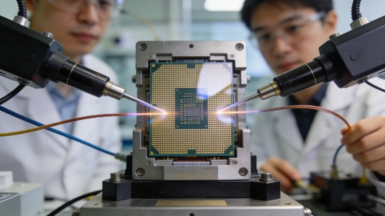
A UCLA research group has demonstrated a semiconductor chip that combines terahertz signal generation and detection, using quantum-well photodiodes and standard fabrication methods, potentially enabling scalable terahertz systems for communications and sensing
Researchers at the University of California, Los Angeles have demonstrated a semiconductor chip that integrates both the generation and detection of terahertz signals, a technical advance that could make terahertz systems more practical for communications, imaging, and sensing. The work, published in Nature Communications, addresses a longstanding barrier in terahertz technology: the need for bulky, expensive, and difficult-to-scale laboratory equipment to generate, manipulate, and detect signals in the terahertz frequency band, which lies between microwaves and infrared light.
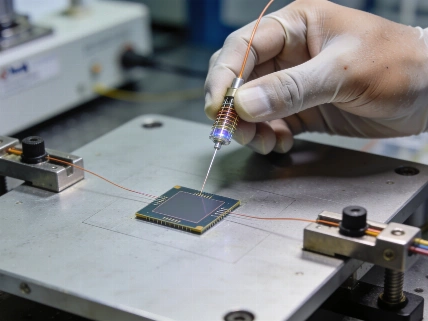
The UCLA-led team focused on integrating multiple terahertz system functions onto a single chip using quantum-well PIN photodiodes fabricated from gallium arsenide and aluminum gallium arsenide (GaAs/AlGaAs). Unlike previous approaches that relied on specialized materials or nonstandard fabrication, the researchers used quantum wells-ultrathin semiconductor layers already common in photonic integrated circuits. This choice allowed them to leverage established industry manufacturing processes, improving the prospects for scalability and commercial viability.
Chip Demonstration and Measured Performance
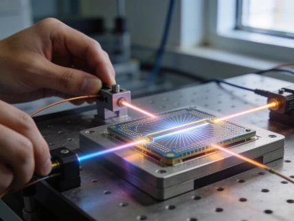
To evaluate the chip, the team directed two laser beams with slightly different frequencies into the quantum-well device. The overlap of these beams produced an electrical oscillation at the difference frequency, which, when tuned to the terahertz range, enabled the device to generate a terahertz signal. The same structure could also detect incoming terahertz waves, demonstrating dual functionality. Measurements showed that electrons escaped the quantum wells in less than a trillionth of a second, fast enough to support terahertz-frequency operation. The prototype achieved frequency-tunable terahertz generation and detection across the 100-500 GHz range. Integration of a semiconductor optical amplifier on the same chip increased terahertz generation efficiency by approximately an order of magnitude and reduced the required optical power for operation.
The system remains at the prototype stage and currently relies on external lasers. However, the platform-referred to as Monolithically Integrated Terahertz Optoelectronics (MITO)-was designed to accommodate future integration of tunable lasers and additional photonic components. The researchers report that all fabrication steps are compatible with commercial photonic foundries, a key requirement for potential large-scale production.
Technical and Practical Limitations
While the demonstration establishes that quantum-well photodiodes can support both efficient terahertz generation and sensitive detection on a single chip, several limitations remain. The prototype depends on external laser sources, and the integration of on-chip lasers and other active photonic elements has not yet been realized. The system has not been tested outside laboratory conditions, and no independent verification of performance or reliability in real-world environments has been reported. The current work does not address long-term stability, manufacturing yield, or the effects of environmental variation on device performance.
Further engineering is required before the technology can support fully integrated terahertz communication or imaging systems suitable for commercial deployment. The team identifies next steps as incorporating additional on-chip components, improving efficiency, and scaling the platform to larger arrays of terahertz sources and detectors. The compatibility with standard photonic manufacturing processes distinguishes this approach from earlier efforts that required specialized fabrication, but the transition from prototype to product remains unproven.
Potential Applications and Context
If the MITO platform can be scaled and reliably manufactured, it could enable compact, manufacturable terahertz systems for wireless communications, portable imaging, chemical sensing, industrial inspection, and remote sensing. The integration of multiple terahertz functions on a single chip could reduce the size, cost, and complexity of current laboratory systems, but practical deployment will depend on further advances in on-chip integration, system robustness, and regulatory approval for new communication bands.
The research stands out for demonstrating both terahertz signal generation and detection on a platform compatible with established photonic manufacturing. However, the evidence is limited to laboratory prototypes, and the technology's performance, safety, and reliability in operational settings remain to be established. No independent replication or external audit of the results has been reported as of publication.
Terahertz systems operate in a frequency range that has long been considered promising for high-speed wireless communication and advanced imaging, but practical deployment has been limited by the complexity and cost of generating and detecting terahertz signals. Integrating these functions onto a single chip using standard semiconductor processes could lower barriers to adoption, but the transition from laboratory demonstration to commercial product typically requires extensive engineering, validation, and regulatory review. The distinction between laboratory prototypes and deployable systems is critical in evaluating the significance of new device architectures in this field.