La Luce Cristallina has introduced a silicon-based quantum paraelectric strontium titanate on insulator wafer platform engineered for quantum computing and cryogenic electronics, with a focus on foundry compatibility and voltage-tunable dielectric control
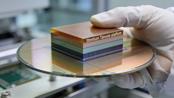
La Luce Cristallina's new quantum paraelectric strontium titanate on insulator (QP-STOI) wafer platform enters the quantum hardware landscape with a clear engineering proposition: enable voltage-tunable dielectric control at cryogenic temperatures on a silicon-compatible substrate. The company claims its 0.5-micrometer-thick strontium titanate (SrTiO3, or STO) layer, bonded atop a thick silicon dioxide insulator, offers a hundredfold increase in thickness over conventional epitaxial STO buffer layers directly grown on silicon. This architecture is designed to support quantum computing, cryogenic electronics, and non-linear electro-optic devices by leveraging the extreme dielectric tunability of STO in its quantum paraelectric regime.
Material System and Device Architecture
The QP-STOI platform is built on a silicon base with a substantial silicon dioxide insulating layer, topped by a bulk-like, highly insulating STO film. At temperatures near liquid helium (below 10 K), STO does not freeze into a ferroelectric state but instead remains quantum paraelectric, meaning its dielectric constant remains exceptionally high and voltage-tunable without domain formation. This property is critical for applications requiring precise phase and frequency control, such as low-noise parametric amplifiers for quantum processor readout, tunable microwave resonators, and electro-optic modulators. The company positions the substrate as fully compatible with standard CMOS and commercial semiconductor foundry processes, targeting integration into existing 200 mm and 300 mm fabrication lines.
Experimental Parameters and Engineering Claims
According to La Luce Cristallina, the QP-STOI wafers are currently available in a 2-inch format for early-stage device prototyping, with plans to scale to 200 mm (8-inch) wafers for commercial production. The STO layer's thickness-0.5 micrometers-marks a significant departure from the sub-10-nanometer buffer layers typically used in silicon-based quantum device research. The company asserts that this increased thickness, combined with the insulating SiO2 base, enables bulk-like dielectric behavior and reduces leakage, which are persistent challenges in thin-film oxide integration. The platform is engineered for operation at cryogenic temperatures, where the quantum paraelectric state of STO allows for strong, voltage-controlled dielectric response without the complications of ferroelectric domain pinning or hysteresis.
Integration and Policy Context
La Luce Cristallina's announcement arrives as national quantum infrastructure initiatives accelerate, including the US Department of Commerce's $2 billion CHIPS Act quantum allocation and the launch of the NIST Quantum Manufacturing Engineering Center. The company's emphasis on foundry compatibility and scalable wafer formats aligns with the push for domestic quantum hardware supply chains and standardized device platforms. While the QP-STOI substrate is positioned as a solution for integrating voltage-tunable dielectrics into quantum and cryogenic circuits, the practical impact will depend on reproducible device performance, yield, and the ability to maintain low noise and high stability across large-scale fabrication. Related efforts to bridge quantum materials and scalable device engineering have also been reported earlier in the context of diamond-based quantum sensors for navigation.
Limitations and Open Questions
No independent benchmarking data or peer-reviewed device demonstrations have yet been released for the QP-STOI platform. Key technical questions remain about interface quality, defect density, and the reproducibility of dielectric properties across full wafers. The transition from 2-inch prototypes to 200 mm commercial wafers will require tight process control to avoid variability that could undermine device performance. The company's claims of full CMOS compatibility and integration into existing foundry lines will need to be substantiated by third-party fabrication and device testing. Until such evidence is available, the QP-STOI platform should be viewed as a promising but unproven substrate for quantum and cryogenic device development.
Quantum paraelectricity describes a regime in certain materials, such as strontium titanate, where quantum fluctuations prevent the onset of ferroelectric order even at very low temperatures. Instead of forming static electric domains, the material's dielectric constant remains extremely high and can be tuned by an applied voltage. This property is valuable for quantum and cryogenic electronics because it enables strong, controllable dielectric response without the noise and instability associated with domain wall motion or hysteresis. However, achieving uniform, defect-free quantum paraelectric films at wafer scale remains a significant materials engineering challenge, and the practical utility of such substrates depends on their integration with low-noise, high-yield device fabrication processes.