
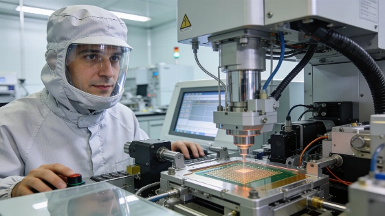
A new quantum nanofabrication area at IMB-CNM in Barcelona brings advanced electron-beam lithography and metrology tools to Spain's largest cleanroom for quantum device prototyping, aiming to bridge laboratory research and industrial pilot lines
Spain has opened the Quantum Nanofabrication Area at the Institute of Microelectronics of Barcelona (IMB-CNM), part of the Spanish National Research Council (CSIC). The facility is described by several scientific outlets, including Euronews, as the country's most advanced research site for making quantum chips and devices. The cleanroom is intended to help move quantum hardware from lab-scale research toward industrial pilot production, a step that institutions like CERN and MIT have also identified as a major challenge in quantum engineering.
Cleanroom expansion and equipment
The upgraded cleanroom includes new fabrication and analysis tools: the EBPG 5150Plus electron-beam lithography system, combined scanning electron microscopy and electron-beam lithography (SEM/EBL) instruments, and atomic force microscopy (AFM) systems. These allow for nanometer-scale patterning and detailed surface analysis, supporting the production of quantum processing units (QPUs), photonic integrated circuits, and quantum key distribution (QKD) components. The facility is set up to address technical bottlenecks that often prevent proof-of-concept devices from becoming scalable, manufacturable systems. According to CSIC, the new area is focused on cleanroom-based prototyping and nanoscale characterization for quantum technologies and advanced microelectronics, not just basic lab research.
More than €6 million for the expansion came from Spain's PERTE Chip program, backed by NextGenerationEU, and the Complementary Plan for Quantum Communications under CSIC. This investment is part of a national strategy to build the infrastructure needed for competitive quantum technology development, similar to efforts at research centers like the Max Planck Society and Stanford University.
National quantum strategy
The cleanroom upgrade is a key part of CSIC's broader quantum technology initiative, led by the new Quantum Advanced Research Center (QuARC-CSIC). QuARC-CSIC brings together 36 research groups from 21 institutes, working on quantum computing and simulation, quantum communications, quantum sensing and metrology, and quantum information theory. The center combines hardware development with algorithmic research, including hardware-algorithm co-design for fermionic quantum simulation. This work recently received a €1.5 million European Research Council Starting Grant to develop atomic quantum simulators for many-body physics, a direction also covered in recent Nature publications on quantum simulation platforms.
By pooling expertise and infrastructure, QuARC-CSIC aims to build a national ecosystem that supports both foundational research and the engineering challenges of quantum device fabrication. Integrating fabrication, measurement, and algorithm development is meant to shorten the path from scientific discovery to practical quantum technologies, following international best practices at places like Harvard and NASA's Quantum Artificial Intelligence Laboratory.
Bridging laboratory and industry
The facility's focus on pre-production quantum hardware addresses a persistent problem: moving from lab prototypes to devices that can be manufactured at scale. The new nanofabrication area is equipped for the iterative process of device design, fabrication, and testing, which is essential for improving yield, reproducibility, and performance in quantum systems. This is especially relevant for quantum processors, photonic circuits, and QKD modules, where device variability and fabrication defects can affect reliability.
Spain's investment in quantum infrastructure follows a wider European trend of building national and regional capabilities for quantum research and development. As reported earlier, European initiatives are increasingly focused on connecting laboratory advances with operational testbeds and pilot production lines to close the gap between research and deployment.
Technical and engineering challenges
Even with the new facility, significant engineering challenges remain. Achieving reproducible nanofabrication at the scale and quality needed for fault-tolerant quantum computing or secure quantum communication is difficult. Device yield, process variability, and integration with cryogenic and control systems still limit the practical use of quantum hardware. The cleanroom's advanced tools provide a platform for tackling these issues, but moving from prototype to scalable system will require ongoing technical progress and careful benchmarking, as discussed in peer-reviewed studies in Science and PNAS.
Spain's approach-combining national investment, coordinated research, and advanced fabrication infrastructure-puts the country in a position to take part in the next phase of quantum technology development. The real test will be whether these resources can produce reproducible, high-performance devices that meet the demands of real-world quantum applications.
Quantum device fabrication depends on precise control of materials and structures at the nanometer scale. Electron-beam lithography allows direct writing of patterns with features smaller than 10 nanometers, which is needed for defining quantum dots, Josephson junctions, or photonic waveguides. Atomic force microscopy provides high-resolution surface analysis, letting researchers detect defects and measure roughness that can affect device performance. The reproducibility and yield of these processes are critical for scaling up from single devices to arrays or integrated circuits. In quantum hardware, even small fabrication imperfections can introduce noise, reduce coherence, or limit gate fidelity, making advanced cleanroom infrastructure essential for progress in the field.