Quobly has signed agreements with TNO and OrangeQS to develop automated, high-throughput testing and metrology for silicon spin qubits on 300 mm wafers, aiming to address device variability and accelerate commercial quantum processor manufacturing
European ambitions for scalable quantum computing hardware took a concrete step forward as Quobly, a French developer of silicon spin qubit devices, formalized two technical partnerships in the Netherlands designed to address one of the field's most persistent bottlenecks: reliable, high-throughput testing and characterization of quantum devices at the wafer scale.
Automated Screening for Silicon Spin Qubits
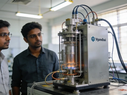
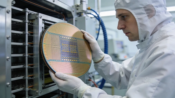
At the heart of the announcement is Quobly's agreement with Orange Quantum Systems (OrangeQS) to adapt the OrangeQS MAX modular cryogenic test platform for semiconductor spin qubits. Originally engineered for superconducting quantum processors, the system will now be configured to automate the measurement and screening of large arrays of silicon quantum dots at cryogenic temperatures. This approach is intended to move beyond manual, device-by-device testing, enabling rapid yield assessment and quality control across entire 300 mm wafers-a scale necessary for any realistic commercial deployment.
The OrangeQS MAX racks are designed to operate at the millikelvin temperatures required for spin qubit operation, integrating automated protocol libraries to execute measurement sequences and extract key performance metrics. By embedding these workflows into the manufacturing pipeline, Quobly aims to identify process-induced variability and device failures early, reducing the risk of undetected defects propagating into larger quantum processor assemblies.
Metrology and Materials Analysis with TNO
In parallel, Quobly has signed a Memorandum of Understanding with the Netherlands Organisation for Applied Scientific Research (TNO) to expand joint research at TNO's Quantum Information Technology Test Facility. The collaboration focuses on advanced device metrology, materials analysis, and stack integration, with a particular emphasis on understanding how substrate properties, process variations, and cryogenic interfaces affect spin qubit coherence and gate fidelity across full wafers.
This partnership leverages TNO's infrastructure to align with Quobly's existing manufacturing ecosystem, which includes STMicroelectronics, CEA-Leti, Soitec, and Air Liquide for isotopically purified silicon-28 supply. The goal is to systematically reduce variability and improve reproducibility, both of which remain major obstacles to scaling up from laboratory prototypes to manufacturable quantum processors.
Wafer-Scale Integration and Industrial Roadmap
Quobly's technical roadmap calls for initial cloud-based deployment of its Alloy product family by late 2026, with a long-term target of reaching one million physical qubits by 2032. The company's recent €115 million Series A financing, closed in June 2026, underscores the scale of investment required to industrialize quantum hardware. The agreements with TNO and OrangeQS are positioned as foundational steps toward integrating device characterization, metrology, and automated testing into a unified European supply chain for silicon spin qubits.
While the company's ambitions are clear, the technical hurdles are substantial. Device yield, process uniformity, and measurement automation are all critical for moving beyond demonstration-scale chips. The need for robust, reproducible testing infrastructure is echoed across the sector, as seen in recent developments in cryogenic interconnects for large-scale quantum processors.
Technical Evidence and Remaining Challenges
Quobly's manufacturing pipeline is built around 300 mm fully depleted silicon-on-insulator (FD-SOI) CMOS wafers, using isotopically purified silicon-28 to minimize nuclear spin noise. The integration with TNO and OrangeQS is intended to provide high-throughput, automated screening of spin qubit arrays at cryogenic temperatures, but the company has not yet released detailed figures on device yield, coherence times, or gate fidelities achieved at scale. The technical documentation available so far describes the infrastructure and workflow, but independent benchmarking of large-scale device performance remains outstanding.
Without transparent, reproducible data on wafer-scale device quality and error rates, claims of scalability remain provisional. The transition from laboratory demonstration to commercial quantum computing will depend not only on the ability to fabricate large numbers of qubits, but also on the capacity to measure, qualify, and control them with sufficient precision to support error correction and useful computation. Until these metrics are published and independently verified, the field remains in a phase of infrastructure build-out rather than demonstrated quantum advantage.
Silicon spin qubits are engineered using the quantum property of electron spin confined in semiconductor quantum dots. Each spin qubit is defined by the orientation of an electron's spin, which can be manipulated using microwave or electric fields and measured via charge sensing or spin-dependent tunneling. The coherence time of a spin qubit-the interval over which it maintains its quantum state-is limited by interactions with the environment, including nuclear spins in the host material and charge noise at interfaces. Isotopically purified silicon-28 reduces decoherence from nuclear spins, but device variability and fabrication defects remain significant challenges. Achieving high-fidelity control and measurement across large arrays is essential for scaling up to practical quantum processors, making automated, wafer-scale testing a critical engineering milestone.