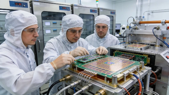
PsiQuantum has secured a $125 million agreement with DARPA to support independent verification of its photonic quantum computing hardware, manufacturing processes, and cryogenic infrastructure as part of the Quantum Benchmarking Initiative
PsiQuantum, a developer of photonic quantum computing systems, has entered a $125 million expanded agreement with the Defense Advanced Research Projects Agency (DARPA) under the Quantum Benchmarking Initiative (QBI). This performance-based contract, the company's largest U.S. government award to date, funds a series of technical audits and validation tasks targeting PsiQuantum's silicon-photonic hardware, integrated photonic manufacturing, and supporting cryogenic systems. The agreement is structured around QBI's Stage C, which emphasizes independent technical verification of utility-scale quantum computing architectures.
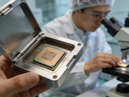
Under the expanded Stage C framework, DARPA technical teams will conduct on-site inspections and component-level testing at PsiQuantum's Milpitas, California facility. The evaluation covers four operational domains: advanced material manufacturing, photonic edge coupling and assembly, system-level cryogenic validation, and algorithmic resource benchmarking. In practice, this means DARPA auditors will directly access PsiQuantum's internal design and manufacturing pipelines, including yield auditing of barium titanate (BTO) thin-film electro-optic modulators, hands-on testing of automated chip-to-fiber optical packaging, and verification of custom cryogenic infrastructure designed to support photonic routing and detector arrays. Live benchmarking of algorithmic resource estimates will be performed using PsiQuantum's proprietary software platform, Construct, which is intended to model resource requirements for fault-tolerant quantum algorithms.
Manufacturing and Infrastructure
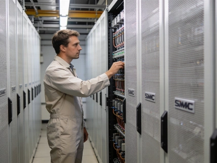
The agreement builds on a previous $31.8 million Stage C award from September 2025, significantly broadening the scope and depth of DARPA's technical evaluation. The expanded funding supports not only device-level inspection but also system-level validation of PsiQuantum's manufacturing processes and cryogenic infrastructure. The company's silicon-photonic quantum chips are fabricated using integrated photonics techniques, with a focus on scalable, high-yield production. The cryogenic systems under review are engineered to maintain stable operation of photonic routing and single-photon detection at temperatures required for low-noise quantum measurement.
In parallel with the DARPA contract, PsiQuantum has signed a Letter of Intent with the U.S. Department of Commerce for $100 million in proposed direct funding under the CHIPS and Science Act, and has received state-level capital commitments in Illinois. These investments are intended to support domestic manufacturing capacity, including PsiQuantum's role as an anchor tenant at the Illinois Quantum and Microelectronics Park (IQMP) in Chicago. However, the technical milestones required for commercial deployment remain subject to independent verification and reproducibility at scale.
Verification and Remaining Challenges
The QBI Stage C process is designed to provide independent assessment of whether a quantum computing architecture can meet the requirements for practical, fault-tolerant computation. For PsiQuantum, this means demonstrating that its photonic hardware, manufacturing processes, and cryogenic systems can deliver the performance, reliability, and reproducibility needed for utility-scale quantum computing. The DARPA-led audits will focus on measurable outcomes, including device yield, optical coupling efficiency, cryogenic stability, and the accuracy of algorithmic resource estimates. While the company's roadmap targets deployment of a commercially useful, fault-tolerant quantum computer before 2033, the current agreement does not establish that such a system has been realized or that all engineering challenges have been overcome.
As of June 2026, the expanded DARPA agreement represents a significant step in subjecting PsiQuantum's claims to external technical scrutiny. However, the results of these audits, including device performance metrics and system-level validation, have not yet been published in peer-reviewed literature or independently replicated by external laboratories. The practical utility of photonic quantum computing at scale remains contingent on overcoming losses, fabrication variability, and the integration of error correction protocols that can operate reliably under real-world conditions.
In the context of quantum computing, the distinction between physical and logical qubits is central to evaluating progress toward fault-tolerant systems. Physical qubits are the actual quantum devices-such as single photons or quantum dots-that can be directly manipulated and measured. Logical qubits, by contrast, are encoded across multiple physical qubits using error-correcting codes to detect and correct errors arising from noise and imperfections. Achieving fault tolerance requires not only high-fidelity physical qubits but also the ability to implement error correction at scale, with logical error rates that decrease as more resources are added. In photonic architectures, this challenge is compounded by optical losses, detector inefficiency, and the complexity of integrating large numbers of components. Independent verification of both physical and logical qubit performance is essential for establishing the viability of any proposed quantum computing platform.