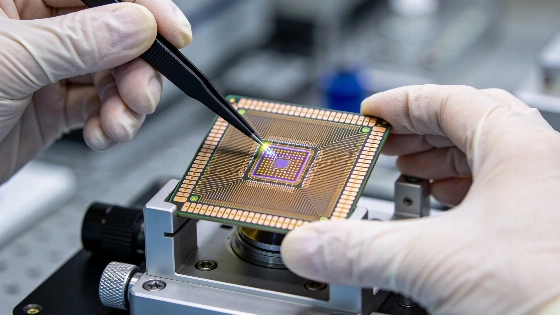
OpenLight and Tower Semiconductor have released a photonic design kit for Cadence EDA tools, enabling engineers to develop high-speed photonic integrated circuits with on-chip lasers for data centers and optical systems
OpenLight, a California-based semiconductor company, and Tower Semiconductor, headquartered in Israel, have announced the expansion of their PH18DA photonics ecosystem with the release of OpenLight's photonic Process Design Kit (PDK) for Cadence electronic design automation (EDA) tools. This development is intended to streamline the design of photonic integrated circuits (PICs) by providing engineers with a unified environment for integrating both active and passive photonic components, including on-chip lasers, modulators, and amplifiers.
Hybrid InP and Silicon Platform Enables Integrated Photonics
The PH18DA platform is built on a combination of indium phosphide (InP) and silicon, a hybrid approach that allows for the integration of active photonic devices directly onto a single chip. Indium phosphide is widely used in high-speed optical communications due to its ability to efficiently generate and detect laser light. By making the PDK available through Cadence's established EDA environment, the companies aim to lower the barrier for engineers developing custom photonic application-specific integrated circuits (PASICs) for data centers, advanced optical interconnects, and sensing applications.
PH18DA Targets 400G and 1.6T Photonic Circuits
According to the companies, the expanded ecosystem is designed to support the development of 400G and 1.6T photonic circuits, which are relevant for next-generation data center infrastructure and high-bandwidth optical links. The integration of active photonic devices within the same design environment as conventional electronic integrated circuits (EICs) is intended to enable co-optimized electro-optical designs, potentially improving performance, power efficiency, and scalability. However, the announcement does not include independent benchmark results or third-party validation of the claimed performance improvements.
Cadence Integration Aims to Simplify Photonic Chip Design
The PDK provides a comprehensive library of verified photonic components, allowing engineers to simulate, design, and prepare layouts for manufacturing on Tower Semiconductor's PH18DA process. This process is positioned as a commercial manufacturing platform, but the companies have not disclosed the number of designs fabricated, yield rates, or operational reliability in field deployments. The integration with Cadence tools is expected to make photonic chip development more accessible to engineers familiar with electronic IC workflows, but the transition from design to volume manufacturing remains subject to the usual challenges of photonic device fabrication, including process variability and packaging complexity.
Optical Interconnects Address Data Center Bandwidth and Power Limits
In the context of broader industry trends, the move toward integrating photonic and electronic components on a single chip reflects ongoing efforts to address bandwidth and energy constraints in data centers. While the PH18DA platform targets high-speed optical interconnects, other companies are pursuing parallel strategies in photonic computing and chiplet-based architectures. For example, recent industrial initiatives have focused on scaling up production of advanced robotics hardware, as seen in efforts to mass-produce humanoid robots for automation, such as the planned rollout of AI-enabled robots at a Kyoto facility.
Manufacturing, Packaging and Reliability Remain Key Challenges
Despite the technical promise of monolithic photonic integration, several limitations remain. The PH18DA platform's compatibility with existing EDA tools may simplify design, but the complexity of photonic device testing, packaging, and long-term reliability still requires specialized expertise. The companies have not released detailed data on device lifetimes, error rates, or field performance, and the impact of process variations on large-scale manufacturing is not yet fully characterized. As with other advanced semiconductor technologies, the transition from laboratory demonstration to robust commercial deployment will depend on continued process optimization and independent evaluation.
How Photonic Integrated Circuits Work
Photonic integrated circuits (PICs) combine multiple optical components—such as lasers, modulators, and detectors—onto a single chip, enabling high-speed data transmission with reduced energy consumption compared to traditional electronic interconnects. Unlike conventional electronic circuits, PICs rely on the manipulation of light rather than electrical signals, which introduces unique challenges in design, simulation, and manufacturing. The integration of photonic and electronic design environments aims to bridge this gap, but successful deployment still depends on precise fabrication, packaging, and system-level validation to ensure reliable operation in demanding applications like data centers and advanced sensing systems.