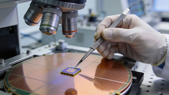
Researchers have demonstrated micro-transfer printing to combine materials like III-V semiconductors and lithium niobate with silicon photonics, addressing integration challenges for faster optical computing and communications hardware
Researchers have reported progress in using micro-transfer printing (MTP) to integrate diverse materials onto silicon photonics platforms, a step that could address longstanding manufacturing barriers in optical computing and communications hardware. The approach, described in a recent peer-reviewed study in the Journal of Lightwave Technology, enables the assembly of components made from materials that cannot be processed using standard CMOS semiconductor fabrication, such as III-V semiconductors and lithium niobate, directly onto silicon-based photonic circuits.
Silicon photonics relies on light to transmit data, offering higher bandwidth and lower latency than conventional electrical interconnects. While silicon-based photonic devices are already deployed in telecommunications and data center networks, their functionality is limited by the material's inability to efficiently generate or modulate light on-chip. Materials like indium phosphide and gallium arsenide can fill these gaps, but integrating them with silicon at scale has proven technically challenging due to incompatibilities in fabrication processes and thermal budgets.
Micro-Transfer Printing Process
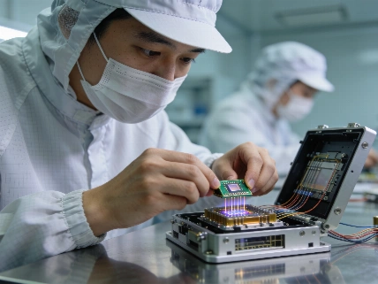
The MTP technique begins with the fabrication of thin-film devices, known as coupons, on a source wafer. A sacrificial layer is selectively etched, allowing an elastomeric stamp to pick up the coupons and transfer them onto a target silicon wafer. The transferred devices are then bonded using adhesive or direct bonding methods. This process allows multiple device types, each optimized using its own fabrication process, to be assembled onto a single silicon photonics platform without requiring high-temperature processing steps that could damage sensitive materials.
Demonstrations to date include the integration of indium phosphide lasers with silicon photonic engines for optical and microwave signal processing, gallium arsenide lasers with silicon nitride waveguides, and narrow-linewidth indium phosphide lasers for coherent communications and lidar. Researchers have also achieved wafer-level integration of lithium niobate modulators with silicon nitride photonic circuits, as well as heterogeneous electronic-photonic optical receiver platforms. These results suggest that MTP can support a range of photonic system architectures beyond a single application domain.
Technical and Manufacturing Challenges
Despite these advances, MTP remains at the research and pilot stage. The reported demonstrations have not yet reached the scale or reliability required for high-volume industrial manufacturing. Key challenges include achieving high manufacturing yield, ensuring long-term reliability of the bonded interfaces, and increasing production throughput. The transition from laboratory-scale assembly to wafer-scale, high-yield manufacturing will require further process optimization and the development of a robust supply chain for source materials and device fabrication.
To address these barriers, the research team has established a pilot manufacturing line focused on scaling up MTP for industrial use. The pilot aims to evaluate process stability, yield, and integration quality under conditions that more closely resemble commercial production. The outcome of this effort will help determine whether MTP can move beyond research demonstrations to support the next generation of silicon photonics hardware for data centers, communications, sensing, and emerging quantum technologies.
In one reported demonstration, researchers successfully integrated indium phosphide lasers onto silicon photonic circuits at wafer scale, achieving device placement accuracy within sub-micron tolerances. However, the overall process yield and long-term reliability metrics have not yet matched those of established CMOS-compatible processes. The study emphasizes that further engineering work is needed before MTP can be considered for routine industrial deployment.
Micro-transfer printing represents a form of heterogeneous integration, where components made from different materials are combined onto a single substrate. Unlike monolithic integration, which requires all materials to be compatible with a single fabrication process, heterogeneous integration allows each component to be manufactured using the most suitable process before assembly. This flexibility is particularly important for photonic systems, where no single material can provide all required optical and electronic functions. However, heterogeneous integration introduces new challenges in alignment, bonding, and quality control that must be addressed to ensure reliable large-scale production.