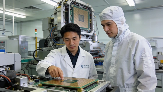
Applied Materials and University of California Berkeley have established the EPIC Center in Silicon Valley to connect academic research with industrial semiconductor manufacturing, aiming to accelerate the development and scaling of new materials and processes for AI chips
Applied Materials and the University of California Berkeley have announced a partnership to establish the EPIC Center in Silicon Valley, a facility designed to address the persistent gap between semiconductor research and commercial manufacturing. The collaboration aims to accelerate the development of new materials and process technologies for AI chips by providing university researchers with direct access to advanced industrial equipment and Applied Materials engineering teams.
In semiconductor development, promising materials and fabrication techniques often remain confined to laboratory settings for years due to the challenges of scaling up for mass production. University labs typically lack access to the same manufacturing tools and process controls used in industry, making it difficult to evaluate whether a research breakthrough can be reliably reproduced at commercial scale. The EPIC Center is intended to bridge this divide by colocating academic researchers and industrial engineers, allowing for earlier identification of manufacturing bottlenecks and reducing the number of development cycles required before a technology is ready for deployment.
Lab-to-Fab Integration
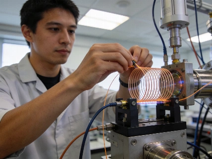
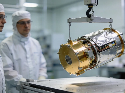
The new center will enable Berkeley faculty and students to work alongside Applied Materials engineers on projects directly relevant to AI computing hardware. By using industry-scale semiconductor fabrication tools, researchers can test whether new materials or processes behave consistently under real manufacturing conditions. This approach is expected to provide earlier feedback on manufacturability, reliability, and process variation-factors that often delay the transition from laboratory demonstration to commercial chip production.
Applied Materials reports that the EPIC Center represents its largest U.S. investment in semiconductor equipment research and development to date. The facility is scheduled to become operational in 2026, with the goal of shortening the time required to move innovations from proof-of-concept to production-ready status. The collaboration builds on existing ties between the two institutions, including shared laboratory facilities and joint research programs in semiconductor technology.
Berkeley's Semiconductor Track Record
UC Berkeley brings a long history of semiconductor research to the partnership. The university established its integrated-circuit prototyping laboratory in 1962 and has contributed foundational technologies such as SPICE, a widely used circuit simulation tool, and FinFET, a three-dimensional transistor architecture now standard in advanced processors. This legacy positions Berkeley as a credible partner for efforts to accelerate the commercialization of new chipmaking methods.
For students and early-career researchers, the partnership offers exposure to industrial-scale equipment and manufacturing practices that are rarely available in academic settings. This experience is expected to improve the practical relevance of university research and help prepare graduates for roles in the semiconductor industry.
Industry Context and Broader Implications
The push to accelerate AI chip development comes as demand for high-performance computing hardware continues to grow. As AI models become larger and more computationally intensive, the need for new materials and manufacturing processes has become a central concern for both industry and academia. The EPIC Center's approach-integrating research and manufacturing environments-reflects a broader trend toward reducing the so-called "lab-to-fab" gap that has historically slowed the adoption of new semiconductor technologies.
Similar efforts to bridge research and production are underway in other sectors of advanced technology. For example, the drive to mass-produce AI-enabled humanoid robots for industrial automation, as seen in recent initiatives by Mitsubishi Motors and Highlanders, highlights the importance of aligning laboratory innovation with scalable manufacturing processes. In both cases, the challenge is not only technical but also institutional-requiring new forms of collaboration between universities, industry, and government to ensure that promising research can be translated into reliable, deployable products.
Applied Materials and Berkeley have not disclosed specific performance targets or evaluation metrics for the EPIC Center's initial projects. However, the facility's focus on AI chip development suggests that early efforts will likely involve materials and process innovations relevant to logic and memory devices used in machine learning accelerators. The effectiveness of the center's approach will depend on its ability to identify manufacturability issues early and to adapt research priorities in response to real-world production constraints.
For the U.S. semiconductor sector, the success of such collaborations may influence the pace at which new AI hardware reaches the market and the degree to which domestic research can be translated into competitive manufacturing capabilities.
Translating laboratory advances in semiconductor technology into commercial products requires overcoming the "lab-to-fab" gap-a set of challenges that arise when moving from small-scale, controlled experiments to high-volume manufacturing. This process involves not only technical hurdles, such as ensuring process repeatability and yield, but also organizational and regulatory factors. Early access to industrial equipment can help researchers identify failure modes and process limitations that are not apparent in academic settings. By integrating research and manufacturing environments, initiatives like the EPIC Center aim to reduce development cycles and improve the reliability of new technologies as they move toward deployment in AI hardware.