Lam Research has announced a $3 billion plan to expand its global semiconductor research labs, aiming to accelerate development cycles and support new chip architectures for advanced computing applications
Lam Research, a major U.S. supplier of semiconductor manufacturing equipment, has announced plans to invest more than $3 billion over five years to expand its global research and development laboratory network. The company says the initiative will increase its experimental capacity by over 50% and is intended to accelerate the pace at which new semiconductor materials, architectures, and manufacturing processes move from laboratory research to commercial production.
The expansion, scheduled to begin in 2026, will add new laboratory sites and technical capabilities across the United States, Asia, and Europe. Lam Research reports that its current network of laboratories supports more than one million experiments annually, with facilities sharing equipment data, research findings, and specialist expertise across time zones. This distributed approach is designed to enable continuous research activity, allowing discoveries at one site to be rapidly shared and built upon at others.
Laboratory Integration and Development Speed
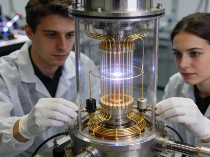
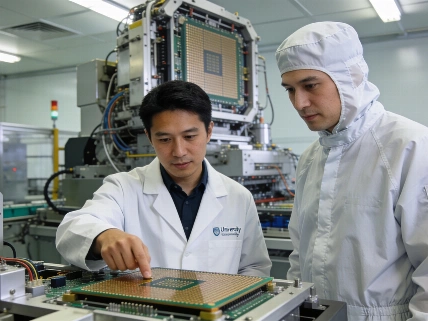
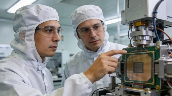
Unlike isolated research centers, Lam Research's laboratories operate as an integrated network. Facilities dedicated to foundational research on new chemicals, materials, and mechatronic systems are linked with process development labs and technology centers located near customer manufacturing sites. According to the company, this structure allows engineers, product developers, and manufacturing teams to work on the same equipment and validate processes in close collaboration with customers' engineering teams.
Lam Research claims that this global integration has enabled process development to proceed up to 2.5 times faster in recent customer projects. The company attributes these gains to the ability to move promising discoveries through multiple stages of development simultaneously, reducing the time required to qualify new manufacturing processes for high-volume chip production.
Technical and Industry Context
The planned investment comes as demand for advanced computing drives the need for new deposition, etching, packaging, and lithography technologies. These processes are critical for producing denser, more power-efficient chips that support artificial intelligence, data centers, and other high-performance computing applications. Lam Research's expansion is positioned as a response to customer requirements for faster development of new chip architectures and manufacturing techniques.
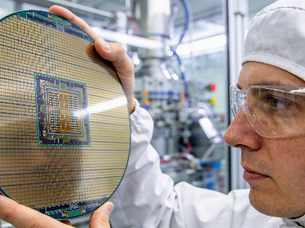
Industry analysts note that wafer-level processing remains central to semiconductor manufacturing, and that increasing investment in research infrastructure is raising expectations for faster qualification of new processes. Lam Research's customers, including major memory and storage manufacturers, have indicated that expanded laboratory capacity could support advances in front-end manufacturing and advanced packaging, both of which are essential for next-generation AI hardware.
Measured Impact and Remaining Questions
Lam Research reports that its laboratories can reduce several weeks of experimental work to a few days in some cases, though these figures are based on internal company data rather than independent audits. The company has not disclosed detailed breakdowns of how the $3 billion investment will be allocated across regions or specific research areas. While the expansion is intended to accelerate product development cycles, the actual impact on time-to-market for new semiconductor technologies will depend on factors including customer adoption, supply chain constraints, and the complexity of emerging chip designs.
No independent verification of the claimed acceleration rates or experimental throughput has been published. The company's announcement does not specify whether the expanded laboratories will incorporate new forms of automation, machine learning, or robotics in their research workflows, nor does it detail any changes to human supervision or safety protocols in laboratory operations.
According to Lam Research, the expansion is expected to help customers qualify new manufacturing processes sooner and scale emerging chip technologies into high-volume production more efficiently. However, the extent to which these improvements will translate into broader industry gains remains to be seen, particularly as semiconductor development cycles are influenced by a range of technical, economic, and regulatory factors beyond laboratory capacity alone.
In the context of semiconductor research, laboratory integration refers to the coordination of experimental work, data sharing, and process validation across multiple sites and teams. By linking foundational research with process development and customer-facing technology centers, companies aim to reduce duplication, accelerate troubleshooting, and move promising innovations more quickly toward commercial deployment. However, the effectiveness of such integration depends on the quality of data exchange, the compatibility of equipment and protocols, and the ability to manage intellectual property and safety risks across jurisdictions.