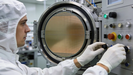
Innolume has ordered a GEN2000 Molecular Beam Epitaxy system from Veeco to increase production of gallium arsenide quantum dot lasers for optical interconnects in AI and cloud data center infrastructure
German photonics manufacturer Innolume has announced the purchase of a GEN2000 Molecular Beam Epitaxy (MBE) system from Veeco Instruments Inc., aiming to expand its capacity for producing gallium arsenide (GaAs)-based quantum dot lasers. The company operates a vertically integrated manufacturing site in Dortmund, Germany, and is scaling up its 6-inch wafer epitaxy and processing lines to meet growing demand for quantum dot (QD) lasers, comb lasers, distributed feedback (DFB) lasers, and semiconductor optical amplifiers (SOAs). These devices are central to optical interconnects and co-packaged optics (CPO) architectures, which are increasingly required for high-bandwidth, low-latency data transfer in artificial intelligence (AI) accelerators and cloud data centers.
Quantum dot lasers differ from conventional quantum well lasers by offering narrower spectral linewidths, reduced threshold currents, and improved thermal stability. These characteristics are particularly relevant for CPO systems, where light sources must operate in close proximity to high-power AI chips and switch ASICs under challenging thermal conditions. The GEN2000 MBE system is designed to enable precise, high-throughput growth of high-density GaAs quantum dot layers, supporting improved wafer uniformity and batch consistency. Alongside the MBE tool, Innolume is also adding a Veeco SPECTOR Ion Beam Deposition (IBD) system to enhance in-house facet coating capabilities, allowing direct application of anti-reflection (AR) and high-reflection (HR) coatings to laser facets.
Manufacturing Scale and Roadmap
The installation of the GEN2000 MBE system is part of a broader expansion strategy at Innolume's Dortmund campus. In parallel, the company is preparing cleanroom facilities for two Riber MBE6000 production reactors, with commissioning targeted for the fourth quarter of 2026. By integrating both Veeco and Riber MBE platforms, Innolume aims to diversify its capital equipment base and increase its 6-inch GaAs wafer production capacity. This approach is intended to address projected demand from hyperscale data center operators, as market research cited by the company suggests that optical transceiver sales for AI infrastructure could approach $80 billion by 2031.
While the GEN2000 MBE system is designed for high-volume epitaxial growth, the actual throughput, device yield, and long-term uniformity will depend on process optimization, material quality, and integration with downstream wafer processing and coating steps. The addition of in-house facet coating is expected to improve control over device performance and reduce reliance on external suppliers, but the impact on overall device reliability and reproducibility will require ongoing evaluation as production scales.
Technical and Engineering Considerations
Quantum dot lasers fabricated on GaAs substrates rely on the controlled deposition of nanometer-scale quantum dot layers, typically using MBE to achieve the required material purity and interface quality. The GEN2000 system supports 6-inch wafer processing, which is a standard size for advanced photonic and semiconductor devices. Achieving high-density, uniform quantum dot layers across large wafers remains a technical challenge, as small variations in growth conditions can affect emission wavelength, threshold current, and device lifetime. The integration of facet coating using ion beam deposition allows for precise control of optical properties at the laser facet, which is critical for minimizing reflection losses and optimizing output power.
According to the company, the expanded facility will be capable of supporting increased wafer throughput and improved batch-to-batch consistency. However, the transition from laboratory-scale fabrication to high-volume manufacturing often introduces new sources of variability, including equipment drift, contamination, and process-induced defects. Device yield and performance uniformity across wafers will be key metrics for assessing the success of the expansion. No independent data on device yield, emission linewidth, or operational lifetime for the scaled-up production has been released at this stage.
Market Context and Remaining Uncertainties
The demand for high-performance optical interconnects is being driven by the rapid growth of AI workloads and the need for energy-efficient, high-bandwidth data transfer within and between data centers. Quantum dot lasers are one candidate for meeting these requirements, but their adoption at scale depends on reliable, reproducible manufacturing and integration with silicon photonics platforms. The roadmap outlined by Innolume includes both Veeco and Riber MBE systems, but the timeline for achieving stable, high-yield production remains subject to engineering and supply chain constraints. The company's projections are based on market research forecasts, which are inherently uncertain and may not reflect actual adoption rates or technical barriers encountered during scale-up.
At present, the expansion represents a significant investment in GaAs-based quantum dot laser manufacturing infrastructure, but the practical impact on device availability, cost, and performance will depend on the outcome of ongoing process development and integration efforts. No independent verification of device performance or manufacturing yield for the expanded facility has been reported. The company's announcement does not specify whether the new systems will be used for research, pilot production, or full commercial deployment, and no peer-reviewed data on device reliability or field performance is available.
Quantum dot lasers are semiconductor devices that use nanometer-scale regions-quantum dots-embedded in a host material to confine charge carriers and control light emission. Compared to quantum well lasers, quantum dot lasers can offer improved temperature stability, lower threshold currents, and narrower emission linewidths, making them attractive for demanding optical communication applications. However, achieving these advantages at scale requires precise control over quantum dot size, density, and uniformity during epitaxial growth, as well as careful integration with downstream processing and packaging steps. The transition from laboratory demonstration to high-volume manufacturing often reveals new sources of variability and error, underscoring the importance of process control and independent performance verification in the development of practical quantum photonic devices.