Xanadu has secured CAD $195 million in federal support to build the Inception facility in Toronto, aiming to advance photonic quantum computing hardware and supply chain integration as part of the CAD $893 million Project OPTIMISM
On August 28, 2026, Xanadu announced a definitive agreement with the Government of Canada to receive CAD $195 million (approximately $140 million USD) in federal funding for the construction of the Inception quantum manufacturing facility in Toronto. This investment, delivered through the Strategic Response Fund and administered by Innovation, Science and Economic Development Canada, forms the largest single government commitment to quantum manufacturing infrastructure in Canadian history. The Inception facility is the central component of Project OPTIMISM, a broader CAD $893 million (about $642 million USD) initiative intended to establish advanced photonic quantum hardware capabilities and domestic supply chain resilience.
Facility Design and Technical Scope
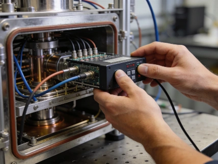
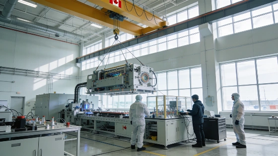
The planned Inception facility will occupy 158,000 square feet in Toronto and is designed to support heterogeneous photonic integration, wafer-level testing, and modular assembly of quantum hardware. Unlike conventional semiconductor foundries, the facility will focus on integrating distinct optical and photonic materials onto scalable chips, a requirement for utility-scale photonic quantum computers. The site will include advanced cleanrooms, continuous wafer-level test stations, and a systems integration center where quantum modules are assembled and verified before deployment. Specialized industrial tooling will be sourced from partners including ASMPT, Bluefors, DISCO, EVG, FiconTEC, and MPI, reflecting the need for equipment beyond standard semiconductor manufacturing lines.
Manufacturing Challenges and Supply Chain Integration
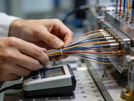
Photonic quantum computing architectures require precise control over photon sources, waveguides, detectors, and packaging, with performance limited by optical loss, fabrication variability, and integration yield. The Inception facility aims to address these challenges by enabling wafer-scale testing and modular assembly, which are essential for scaling up from laboratory prototypes to deployable quantum modules. The facility's advanced packaging capabilities are also expected to support adjacent sectors such as AI hardware, telecommunications, and precision sensing, but the primary focus remains on quantum data center hardware. According to the project plan, the facility is projected to create 275 high-skilled engineering and technical jobs in the Etobicoke-Lakeshore area of Toronto.
Policy Context and Economic Impact
The CAD $195 million federal allocation completes the government's portion of a previously outlined CAD $390 million public support framework for Project OPTIMISM. The investment is positioned as a strategic move to advance Canada's National Quantum Strategy and Defense Industrial Strategy by establishing domestic manufacturing capacity for quantum technologies. Ministers Evan Solomon (AI and Digital Innovation) and Mélanie Joly (Industry) emphasized the role of the project in securing supply chain sovereignty for critical quantum hardware. While the facility's construction and equipment procurement represent a significant infrastructure commitment, the practical impact on quantum computing capability will depend on the reproducibility, yield, and integration quality achieved in manufacturing. For context, other national quantum initiatives have focused on different aspects of quantum technology; for example, the National Science Foundation in the United States has funded institutes to advance quantum sensing for biomedical applications, as described in recent coverage of quantum sensor research funding.
Remaining Engineering and Scalability Questions
While the Inception facility is intended to serve as a global hub for photonic quantum hardware, several engineering challenges remain unresolved. Achieving high-yield heterogeneous integration at wafer scale, minimizing optical loss, and ensuring reliable modular assembly are all critical for moving beyond laboratory-scale demonstrations. The facility's success will depend on the ability to produce quantum modules with reproducible performance, low error rates, and compatibility with fault-tolerant architectures. At present, no public data are available on the expected device yield, integration fidelity, or error rates for the planned hardware. The project's impact on practical quantum computing will ultimately be determined by the facility's ability to deliver high-quality, scalable photonic devices that meet the demanding requirements of error-corrected quantum computation.
Photonic quantum computing relies on encoding quantum information in individual photons, which are manipulated and measured using integrated optical circuits. Unlike superconducting or trapped-ion qubits, photonic qubits can operate at room temperature and are naturally suited to networking, but they face significant challenges in loss, detection efficiency, and large-scale integration. Heterogeneous integration refers to the process of combining different material systems-such as silicon, indium phosphide, and lithium niobate-on a single chip to optimize photon generation, routing, and detection. Achieving high-yield, low-loss integration at scale is a major engineering barrier for photonic quantum computers, and progress in this area is essential for realizing practical, fault-tolerant quantum systems.