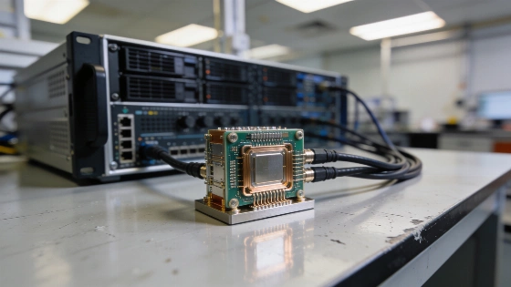
Quobly will use CEA-Leti's FAMES Pilot Line in Grenoble to prototype 3D integration and cryogenic control layers for 300 mm silicon spin-qubit processors, while Alloy Forge and qBraid Cloud offer developers an interim environment before planned access to the Alloy Pioneer QPU.
Quobly has secured direct access to a European pilot line that could determine whether its silicon spin-qubit design can move beyond exploratory fabrication. The agreement with CEA-Leti gives the company a prototyping route for 3D integration and cryogenic control electronics on 300 mm wafers while its commercial manufacturing relationship with STMicroelectronics remains in place. Quobly also describes a wider industrial network involving CNRS, Air Liquide, Soitec and Orano.
Quobly's QSOI(R) architecture places silicon spin qubits directly on a 300 mm fully depleted silicon-on-insulator CMOS substrate. The intended device combines arrays of spin qubits with control electronics operating at cryogenic temperatures on a unified die. That is a demanding integration problem: the quantum elements must be controlled and read out while the surrounding CMOS circuitry is manufactured using processes compatible with very large-scale semiconductor production.
The FAMES Pilot Line is hosted at CEA-Leti in Grenoble under the Chips JU initiative, with support from Horizon Europe, Digital Europe and national authorities participating in the programme. Its facilities cover processing associated with FD-SOI, embedded non-volatile memory, RF functions, power-management integrated circuits and 3D and heterogeneous integration, an area for which CEA-Leti is identified as a lead organisation. The pilot line has also been discussed as a European-scale infrastructure with a budget of about €830 million, spanning FD-SOI, RF, power management and 3D integration. Details of the programme are described by the FAMES Pilot Line.
Quobly's access is therefore not a claim that a fault-tolerant processor has been completed. It is access to infrastructure for testing the manufacturing and packaging steps that a larger processor would require. In semiconductor terms, a 300 mm wafer indicates compatibility with an industrial format; it does not by itself establish high quantum-device yield or uniform performance across the wafer.
The immediate technical value lies in bringing control functions closer to the qubits. Shorter and more integrated signal paths could help manage wiring and control density, but the announcement provides no measured improvement in gate fidelity, readout fidelity, coherence, device yield or operating temperature. Those missing measurements matter more than the wafer diameter when judging whether the architecture can support useful computation. The same distinction is central to how institutions such as MIT and journals including Nature separate a fabrication milestone from a demonstrated computational advantage.
FAMES fills a specific gap between laboratory development and commercial foundry runs. Quobly can use the pilot line to explore process flows for 3D integration and RF control layers before transferring more mature designs into its manufacturing partnership with STMicroelectronics. That staged approach reduces the risk of treating a promising device layout as if it were already a reproducible production process.
The company also points to embedded non-volatile memory as part of the infrastructure it can use while developing next-generation quantum processing units. In this context the memory is an integration capability rather than evidence of a quantum advantage. The available material does not report a benchmark, a completed processor demonstration or a comparison with a classical system.
The distinction is important because a 300 mm line can improve manufacturing relevance without automatically improving the quantum behaviour of each device. Interface disorder, charge noise, fabrication variation, crosstalk, calibration drift and the thermal load from control electronics can all limit a spin-qubit array. None of those quantities is reported here, so the announcement establishes an engineering pathway rather than a performance result.
On 22 September 2026, Quobly announced integration of its Alloy Forge emulator with qBraid Cloud. The environment is described as modelling a 15-qubit linear spin-qubit array on 300 mm FD-SOI CMOS and supporting native two-qubit RZZ interactions. This gives developers a way to test circuits and application concepts against a representation of the proposed hardware model before commercial access to an Alloy Pioneer QPU.
The cloud deployment changes the practical emphasis from a laboratory-only demonstration to application development, but an emulator is not a physical processor. It can expose software, connectivity and compilation issues, while it cannot establish the coherence, calibration stability, leakage behaviour, fabrication yield or noise correlations of manufactured qubits. Results obtained in Alloy Forge should therefore be treated as pre-hardware validation rather than experimental evidence from a QPU.
Quobly plans to offer initial cloud availability for its first-generation Alloy Pioneer processor family by late 2026. In the same September update cycle, the company was reported as targeting VLSI silicon quantum processors with up to one million qubits by 2032. Both dates are plans rather than demonstrated milestones, and the announcement does not specify the number of physical qubits, logical qubits, error-correction code, circuit depth or classical decoding system involved.
Cloud availability would make a processor accessible remotely, but it would not by itself establish useful quantum computation. A credible assessment would need the hardware platform's active qubit count, connectivity, gate and readout performance, calibration stability, runtime and verification method. The broader issue is captured in an earlier analysis of why architecture and error correction matter more than a raw qubit total.
For silicon spin qubits, integration is not a secondary manufacturing detail. The architecture depends on fitting quantum devices and control infrastructure into the same scaling logic used by advanced CMOS while preserving the conditions needed to manipulate individual electron spins. FAMES can test whether that combination is manufacturable; it cannot, by itself, show that the resulting processor will outperform classical hardware or sustain fault-tolerant operation.
The concrete result is institutional and technological: Quobly now has direct access to CEA-Leti's FAMES Pilot Line as an intermediate prototyping environment, alongside its commercial manufacturing partnership with STMicroelectronics. The relevant scale is 300 mm FD-SOI, the integration targets are 3D structures and RF control layers, Alloy Forge models a 15-qubit linear array with native RZZ interactions, the first cloud-access plan is set for late 2026 and the longer-term million-qubit target is set for 2032.
That is meaningful progress in the supply chain for silicon quantum hardware, but it is not evidence that the central quantum-engineering problems have been solved. The announcement supplies no experimental data on qubit performance and no independent verification of a processor. Its strongest claim is narrower and more credible: Quobly is building a bridge from device research toward foundry-compatible prototyping. That bridge is essential, yet the distance from a pilot line to a reliable fault-tolerant machine remains the part that still requires proof.
A physical qubit is an individual controllable quantum system, while a logical qubit encodes information across multiple physical qubits to detect and correct errors. Adding more physical devices does not guarantee more useful logical qubits because control errors, readout errors and connectivity can overwhelm the code's protection. This is why research communities spanning semiconductor laboratories, MIT and peer-reviewed venues such as Nature evaluate scaling claims through error rates, logical performance and reproducibility rather than qubit count alone. On the evidence available here, Quobly has taken a serious step toward testing its architecture at wafer scale, but it has not yet demonstrated scalable quantum performance.