Researchers at the National Institute of Standards and Technology have demonstrated a superconducting nanowire single-photon detector with a 100-micrometer active width, addressing fabrication and noise challenges that have limited quantum photonic hardware
The National Institute of Standards and Technology (NIST) has experimentally demonstrated a superconducting nanowire single-photon detector (SNSPD) with an active width of 100 micrometers, a scale 100 times wider than conventional SNSPDs. This advance, published in Optica, addresses longstanding fabrication and performance bottlenecks in quantum photonic hardware by introducing a magnetic shielding architecture that suppresses edge-induced noise and enables standard microfabrication techniques.
Device Architecture and Measurement
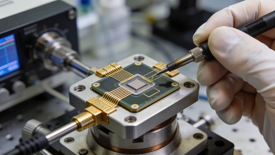
Traditional SNSPDs rely on nanometer-scale superconducting wires, typically around 100 nanometers wide, to detect single photons with high efficiency. However, increasing the width of these wires has historically led to a dramatic rise in dark counts-false detection events triggered by thermal or magnetic fluctuations-due to current crowding at the wire edges. The NIST team implemented a design in which current-biased niobium rails are placed parallel to a central tungsten-silicide (WSi) strip. These rails generate a magnetic self-field that cancels the perpendicular field at the strip edges, redistributing current density toward the center and suppressing the entry of magnetic vortices that cause dark counts.
In laboratory tests, the wide SNSPD achieved a 1010-fold reduction in dark count rate compared to unshielded devices, while maintaining near-unity detection efficiency at mid-infrared wavelengths around 4 micrometers. The device also demonstrated an extended detection plateau at 1550 nanometers, a key wavelength for quantum communication. The architecture is compatible with standard optical photolithography, eliminating the need for electron-beam lithography and its associated yield limitations.
Engineering and Scalability Implications
By enabling SNSPDs with widths up to 0.1 millimeters, the NIST approach removes a major barrier to scaling quantum photonic systems. Wider detectors simplify optical alignment and packaging, reduce sensitivity to polarization, and allow for the fabrication of dense two-dimensional arrays. This is particularly relevant for quantum key distribution networks and photonic quantum processors, where large numbers of detectors must be integrated with minimal loss and high uniformity. The compatibility with established microfabrication processes also supports higher device yields and lower production costs, addressing a key challenge for industrial deployment.
These advances build on recent efforts to address quantum hardware bottlenecks across the industry. For example, the shift in quantum leadership priorities discussed in this analysis of quantum sector leadership changes highlights the growing focus on manufacturability and system integration as quantum technologies move closer to practical deployment.
Noise Suppression and Physical Limits
The core technical challenge addressed by the NIST design is the so-called Pearl limit, where the Meissner effect in superconductors forces current to concentrate at the edges of wide strips, lowering the energy barrier for vortex entry and increasing noise. By actively canceling the edge magnetic field, the new architecture allows the SNSPD to operate near the intrinsic performance limit of the superconducting material, reducing the minimum photon energy required to trigger a detection event. This enables high-efficiency photon detection across a broader wavelength range, including the mid-infrared, which is important for emerging quantum sensing and communication applications.
While the results represent a significant step toward scalable quantum photonic hardware, further work is needed to validate device performance across large arrays, assess long-term stability, and integrate these detectors into complete quantum systems. The reported performance metrics are based on laboratory prototypes, and independent replication will be important for establishing reproducibility and manufacturability at scale.
Remaining Challenges and Outlook
Despite the demonstrated improvements in width scaling and noise suppression, several engineering challenges remain. Integrating wide SNSPDs into complex photonic circuits will require careful management of thermal loads, wiring density, and cryogenic operation. The impact of device-to-device variability, long-term reliability, and system-level losses must also be evaluated as the technology moves from laboratory demonstration to industrial application. Additionally, while the elimination of electron-beam lithography simplifies fabrication, maintaining uniform superconducting properties across large wafers will be essential for high-yield production.
As quantum photonic systems continue to evolve, advances in detector architecture such as the NIST wide-SNSPD will play a critical role in enabling larger, more reliable, and more cost-effective quantum networks and processors. The ability to fabricate high-performance single-photon detectors using standard microfabrication techniques marks a meaningful step toward practical quantum technologies, but the transition from prototype to scalable system will depend on continued progress in integration, reproducibility, and system engineering.
Single-photon detectors are essential components in quantum communication, sensing, and computing. An SNSPD operates by biasing a superconducting wire just below its critical current; when a photon is absorbed, it creates a localized hotspot that drives the wire normal, producing a measurable voltage pulse. The efficiency and noise performance of SNSPDs depend on material properties, device geometry, and operating conditions such as temperature and magnetic environment. Edge effects and vortex entry have historically limited the width of these detectors, constraining both performance and manufacturability. The NIST architecture demonstrates that active magnetic field management can overcome these limits, but scaling to large, reliable arrays will require further engineering advances and independent validation.