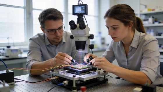
A modular nanopositioning test system developed by SmarAct and Akhetonics enables precise optical and electro-optic characterization of advanced photonic integrated circuits, addressing key engineering challenges in scalable optical computing hardware
Efforts to realize practical optical computing have increasingly focused on the integration and precise characterization of photonic integrated circuits (PICs), which promise high bandwidth and energy efficiency for data processing. In a recent collaboration, German companies Akhetonics and SmarAct have developed a custom test platform designed to address the measurement and alignment challenges that arise when evaluating next-generation PICs for optical processors.
Nanometer-Scale Alignment for Photonic Chips
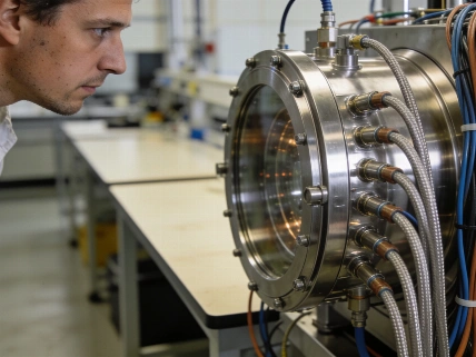
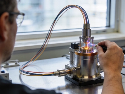
The test system centers on two nanopositioning subsystems, each engineered for multi-axis precision. The first subsystem provides horizontal translation along the X and Y axes and rotation about the Z axis, while the second enables vertical translation and angular adjustment around the X and Y axes. Both subsystems employ SmarAct positioners with integrated optical encoders, achieving a positional repeatability of ±40 nanometers for linear axes and angular control within a few degrees. This level of control is essential for aligning optical fibers with on-chip waveguides, where even a micrometer-scale mismatch can introduce significant coupling losses.
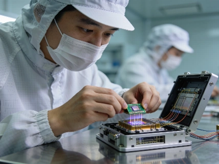
To support comprehensive device evaluation, the platform incorporates a digital microscope for visual inspection and alignment, as well as two independent XYZ probe towers for electrical contact. This configuration allows Akhetonics to perform both optical and electro-optic measurements on PICs, including insertion loss, wavelength- and polarization-dependent coupling, and the characterization of on-chip modulators and photodetectors. The system's modularity and software integration—enabled by SmarAct's Control and Process Environment (SCoPE) with Python scripting—allow for the development of custom calibration and alignment routines, supporting both research and small-batch production workflows.
In practical terms, the test platform enables Akhetonics to map large grids of test components across a PIC, rapidly evaluating device performance and identifying sources of loss or misalignment. The system's travel ranges—49 mm in X and Y, 31 mm in Z, and full 360° rotation—accommodate a variety of chip sizes and layouts. The ability to achieve sub-100 nm alignment precision is particularly important for on-chip optical testing, where coupling efficiency is highly sensitive to positional error. For electrical probing, the system supports contact pads as small as 100 μm × 100 μm, with alignment precision an order of magnitude better than the pad size.
Combining Photonic Design and Precision Engineering
The collaboration between Akhetonics and SmarAct began following discussions at a European photonics conference, with both companies contributing complementary expertise: Akhetonics in photonic design automation and system architecture, and SmarAct in nanopositioning, metrology, and automation. The engineering teams iterated on 3D CAD models and performance requirements before finalizing the system design. Akhetonics then integrated the nanopositioning modules with its own optical and electrical measurement equipment, as well as custom software routines for device characterization.
Python-Based Automation and Custom Workflows
Software flexibility is a key feature of the platform. SmarAct's SCoPE environment provides a modular interface for process automation, device control, and data visualization, supporting both standard and custom workflows. The Python backend allows users to extend functionality, integrate third-party devices, and develop application-specific routines for calibration and alignment. This approach is intended to support the transition from laboratory R&D to scalable manufacturing, although the current system remains a prototype rather than a production-ready solution.
While the test platform addresses critical alignment and measurement challenges, several engineering hurdles remain before large-scale optical processors can be realized. These include the reproducibility of PIC fabrication, integration of active and passive components, and the management of optical loss and crosstalk at scale. The current system demonstrates that precise, automated characterization is feasible for advanced PICs, but further work is needed to translate laboratory prototypes into manufacturable, reliable hardware for high-performance computing applications.
Why Nanopositioning Matters for Optical Computing
Recent advances in experimental physics have highlighted the importance of direct measurement and control in understanding complex systems. For example, extracting physical parameters from a black hole event horizon using gravitational wave data, as described in a recent Science Report article, demonstrates how new instrumentation and analysis methods can provide access to previously inaccessible regimes. In photonics, similar progress depends on the ability to characterize and optimize devices at the nanometer scale, where small errors can have outsized effects on system performance.
Nanopositioning is central to the precise alignment required in photonic device testing. In this context, nanopositioning refers to the ability to control the position of a component—such as an optical fiber or probe tip—with nanometer-scale accuracy and repeatability. Achieving this level of control typically involves piezoelectric actuators, optical encoders, and feedback systems that compensate for drift, vibration, and thermal expansion. In photonic integrated circuits, where optical modes are confined to sub-micrometer waveguides, even small misalignments can lead to significant insertion loss or measurement error. As photonic systems become more complex and integration density increases, the demands on nanopositioning and automated alignment are likely to grow, making robust, flexible test platforms an essential part of the development pipeline.