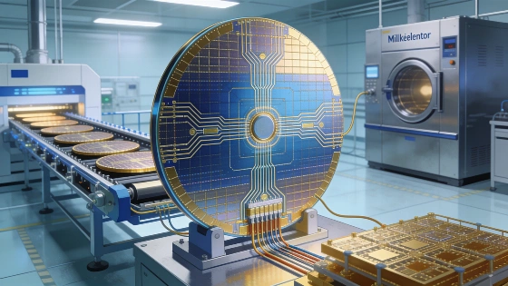
Europe's six quantum pilot lines need shared wafer access, packaging, cryogenic testing and predictable legal pathways if the region is to move from prototype demonstrations to reproducible industrial manufacturing.
Europe has pilot lines for six quantum hardware platforms but still lacks a defined route from prototype chips to production-grade fabrication. The European Quantum Industry Consortium (QuIC) is urging lawmakers to make that industrial bridge a central feature of the European Commission's Chips Act 2.0 proposal, COM(2026) 504.
Presented by the European Commission on 3 June 2026, Chips Act 2.0 has entered the ordinary legislative procedure. The proposal expands "first-of-a-kind" strategic projects across the value chain, creates a dedicated photonics direction and seeks to move quantum chips beyond pilot lines toward prototyping and manufacturing. For qualifying projects, permits would be handled through a national one-stop shop with a maximum stated duration of 12 months. The regulation itself contains little dedicated financing, with major funding decisions expected through the EU's 2028-2034 budget and the European Competitiveness Fund.
QuIC's whitepaper response accepts the value of the six existing EU quantum pilot lines: SUPREME for superconducting systems, SPINS for spin devices, P4Q for photonics, DIREQT for diamond, Q-PLANET for neutral atoms and CHAMP-ION for trapped ions. Its objection is narrower and more consequential. Pilot capability does not by itself provide repeatable commercial fabrication, packaging, testing or access for companies that cannot operate their own semiconductor plants.
Most European quantum hardware firms use neutral process foundries rather than private fabrication facilities. That leaves access to commercial-grade quantum manufacturing dependent on voluntary terms that can be revoked and are set outside the Union. QuIC argues that this is a supply-chain weakness as much as a technology problem because a promising device design is not enough if its process route is unavailable when the design reaches maturity.
The international market is moving in the opposite direction. In the United States, Anderon has described a 300-millimetre wafer manufacturing platform, initial offerings for superconducting qubits and quantum input/output, and the development of process design kits. The company has also reported a completed $1 billion U.S. Department of Commerce CHIPS Act grant alongside a further $1 billion IBM investment. The reported model uses 300-millimetre capacity at the Albany NanoTech Complex rather than relying on construction of an entirely new standalone plant; the federal award is described as a research-and-development commitment under the CHIPS and Science Act, not as a venture round or a disclosed company valuation.
IonQ completed its acquisition of SkyWater Technology on 31 July 2026 in a transaction valued at $1.8 billion. The deal gives IonQ a U.S. manufacturing base while SkyWater continues to operate as a foundry for external customers. It therefore combines vertical integration with continued commercial foundry services rather than eliminating the supplier model altogether.
These developments do not prove that Europe cannot build competitive quantum hardware. They do show the scale and direction of industrial consolidation that European policymakers must address if the region wants control over critical fabrication routes rather than relying on access negotiated with external suppliers. IndustriAll Europe has similarly argued that Chips Act 2.0 should cover the full chain, including research, design, equipment, materials, wafer production, advanced packaging, assembly, testing and end uses.
The issue also connects manufacturing policy with the performance claims made for future quantum systems. A processor roadmap can specify more devices or better control, but it cannot remove wafer variability, packaging constraints, cryogenic wiring, calibration demands or the need to characterize large numbers of components. As an earlier analysis noted in a different context, useful quantum technology depends on the engineering path between a target and a demonstrated system.
That distinction is central to fault-tolerant computing. Logical qubits are built from many physical qubits, and their usefulness depends on error rates, connectivity, control stability and repeated syndrome measurements rather than on the raw number of devices alone. A Nature surface-code study illustrates why scaling and error suppression must be evaluated together: a manufacturing strategy has to support uniform devices and reliable interconnects, not merely isolated laboratory demonstrations.
QuIC recommends extending Article 19 strategic-project status to quantum foundries. The proposed designation would create a legal framework for quantum manufacturing facilities once their processes reach industrial maturity rather than leaving such facilities outside the strategic-project structure used by the Chips Act.
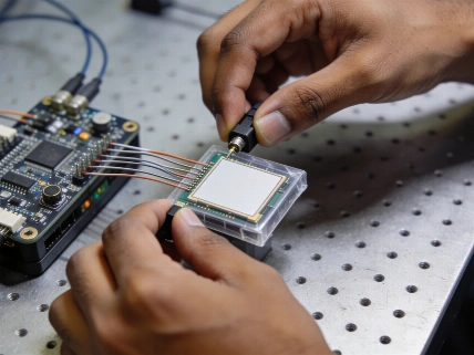
The consortium also calls for a subsidized European multi-project wafer program. An MPW shuttle places designs from multiple users on shared fabrication runs, lowering the entry cost for startups and small and medium-sized enterprises. For quantum developers this would provide a practical route to test process design kits and iterate hardware without immediately financing a dedicated foundry.
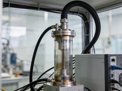
Shared infrastructure would need to continue beyond wafer fabrication. QuIC proposes funding cryogenic testing, high-volume characterization and advanced packaging across the 2 K, 4 K and millikelvin ranges. Those temperatures cover different classes of quantum hardware and measurement requirements; they are not interchangeable labels for one generic cooling problem.
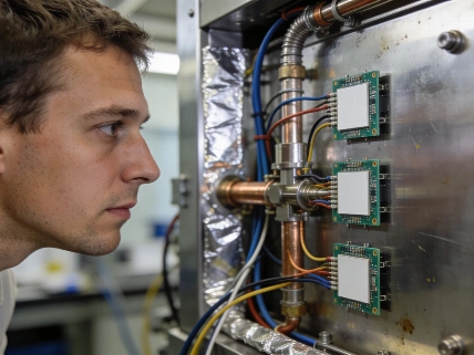
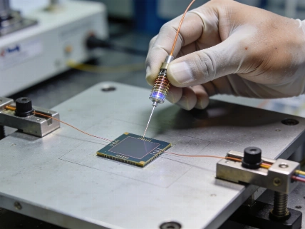
Packaging and characterization determine whether devices can be connected, cooled, controlled and measured consistently. Without that layer, a pilot line can demonstrate that a structure can be fabricated while offering little evidence that a population of devices can be assembled into a stable system. The same principle is familiar from large-scale instrumentation at CERN and from highly integrated engineering programs associated with MIT: subsystem reproducibility is a prerequisite for system-level performance.
QuIC wants the Chips Act's photonics objectives expanded beyond near-infrared telecom wavelengths. Its proposed range includes visible light from 400 to 800 nanometres and deep ultraviolet light from 295 to 325 nanometres, which the consortium identifies as relevant to trapped-ion and neutral-atom architectures.
The recommendation is specific to the hardware. Trapped-ion and neutral-atom systems depend on optical control and therefore require photonic components that are not covered by a policy framework focused mainly on communications wavelengths. Treating photonics as a single category would miss those system-level requirements. Research ecosystems such as the Max Planck Society have helped demonstrate the scientific importance of precision optical control, but industrial policy must also address the manufacturability, packaging and lifetime of the components that provide it.
QuIC further asks policymakers to create accessible designations for small-scale and in-house fabrication routes that can deliver rapid turnaround without meeting the strict "first-of-a-kind" requirement. That proposal recognizes a gap between laboratory fabrication and a billion-euro-class foundry: many quantum companies need repeatable small batches and fast process feedback before they need high-volume production.
The consortium also calls for structural alignment between Chips Act 2.0 and the forthcoming EU Quantum Act. In QuIC's division of responsibilities, the Chips Act would cover chip-level fabrication and process design kits while the Quantum Act would address systems, software, standards and public procurement. That separation could work only if the two frameworks share a practical definition of the interfaces between a manufactured device and the system built around it.
Q-PLANET illustrates how such implementation could begin. The initiative entered its implementation phase three months after its Brussels launch and is planned as a three-year program supported by the EU Chips Joint Undertaking together with national and regional authorities. Its progress will be relevant not only to neutral-atom manufacturing but also to the broader question of whether European pilot-line investments can become durable industrial capacity.
Multi-project wafers are not fault-tolerant quantum computers and a pilot line is not a commercial foundry. They are infrastructure for reducing the distance between a device concept and a reproducible manufacturing process. QuIC's proposal is therefore best read as an industrial test for Chips Act 2.0: unless Europe funds shared access, cryogenic and packaging capacity, and wavelength coverage suited to its hardware platforms, its quantum strategy will support prototypes without securing the production routes those prototypes require.