Anderon has opened licensing for a design kit based on IBM's superconducting qubit process. Its Albany facility has handled more than 10,000 300mm wafers, but the release reports no qubit performance data
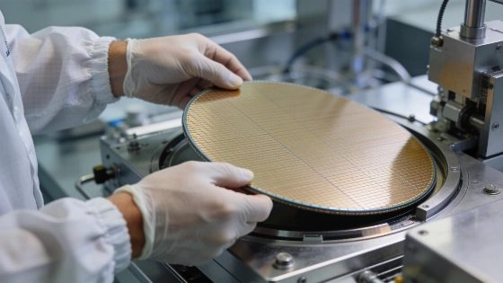
At the Albany NanoTech Complex, Anderon operates a 150,000-square-foot cleanroom for 24/7 wafer processing. The company says its new design kit is intended to help quantum hardware teams move superconducting-device designs onto that 300mm manufacturing line.
Anderon is being established as a standalone, for-profit quantum foundry led by Mukesh Khare, a former IBM executive. The business model is to let quantum-device developers design hardware while a specialist manufacturer fabricates it, rather than requiring each company to build and operate its own production facility. IBM is providing equipment and personnel, while Albany NanoTech supplies the buildings and Anderon owns and operates the equipment, according to RuntimeWire's report.
What the kit provides
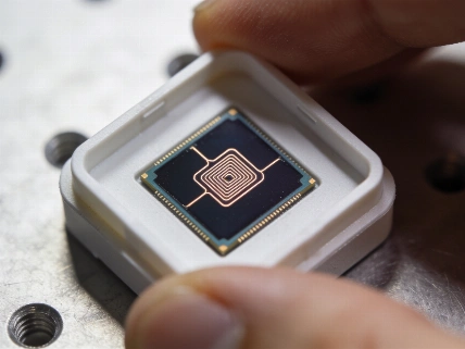
A Process Design Kit, or PDK, gives designers a set of manufacturing constraints and models to work with before a device is fabricated. Anderon's release includes design rules and component models. It also supplies verified building blocks intended to connect custom device design with industrial-scale production.
The kit includes electromagnetic parameters for designers to use in their work. Structural shielding models and baseline reference designs are also part of the release. These resources can make a design process more consistent, but the announcement does not report that a customer device has been built or tested using the PDK.
The initial kit is based on IBM's superconducting qubit process, which Anderon says it has licensed. Anderon describes the PDK as available through licensing agreements handled by its commercial team. No device-level measurements accompany the announcement: it gives no qubit count, yield, fidelity, coherence time, or operating temperature.
A manufacturing base
Anderon was formed as a standalone for-profit quantum manufacturing enterprise backed by $2 billion in funding and support from the U.S. Department of Commerce. On September 16, 2026, the federal CHIPS Act award was finalized at $1 billion, with IBM providing a further $1 billion for the 300mm quantum foundry in Albany. The combined funding is intended to establish manufacturing capacity for Anderon and external quantum-hardware developers.
The Albany site has a longer history as a semiconductor research campus. IBM presented a 2nm semiconductor prototype there in 2021, and the complex hosts advanced-process research involving IBM, Micron and Tokyo Electron. In 2024, the U.S. Department of Commerce designated Albany NanoTech the first flagship research center under the CHIPS Act program and allocated about $825 million for an EUV lithography research center. That earlier funding supports the site's research infrastructure and is separate from the $1 billion federal award for Anderon, as reported by ChosunBiz.
The company says the Albany NanoTech Complex has processed more than 10,000 300mm superconducting wafers over the past few years. Anderon plans to buy additional equipment with funding from the U.S. Department of Commerce and IBM. Some purchases are meant to add processing capabilities that were previously unavailable; others would support higher throughput and equipment redundancy.
Those figures describe infrastructure and processing history, not the number of working qubits or the quality of finished devices. The release does not provide wafer yield, device-to-device variation, or results from a production run using the newly released kit. Without those measures, the PDK's practical effect on fabrication remains unquantified.
Scale and its limits
Anderon expects to work with customers on possible variants of the initial process, tailored to particular device architectures. The company also wants to support other modalities, including semiconductor-based spin qubits. These are future plans, rather than capabilities established by the current PDK.
The company says other quantum hardware developers have wafer-processing facilities, but characterizes them as low-volume development operations. It sees a role for a dedicated foundry in higher-volume production. Rigetti and Google have indicated they might consider working with dedicated production foundries for future high-volume needs; the source does not describe a completed customer agreement.
Anderon argues that higher wafer volumes can reduce costs through economies of scale and use of 300mm wafers rather than 200mm wafers. It also points to potential quality and cycle-time benefits from running a process frequently enough to keep tighter control. Those are manufacturing rationales, not reported comparisons of Anderon's costs, defect rates, or cycle times.
If demand grows beyond the current facility, Anderon says it could need additional capacity in a few years, potentially through a second fab and further financing. For context on a different part of quantum hardware development, Google's decoder simulations addressed error processing, while Anderon's announcement concerns fabrication infrastructure.
A PDK is a design aid, not a guarantee that a device will meet its intended specifications after fabrication. Its models and rules help designers account for a foundry's process, while measurements on fabricated devices are still needed to establish performance and consistency. Anderon's kit is available by licensing agreement.