
Qualcomm Technologies and Amazon are partnering to develop custom silicon and high-speed optical connectivity for AI data centers, aiming to speed up AI inference and data transfer at scale.
Qualcomm Technologies and Amazon have announced a partnership to develop a new class of AI data center infrastructure. The collaboration, made public on September 8, 2026, focuses on building custom silicon and high-performance optical connectivity for large-scale artificial intelligence workloads. Both companies describe the effort as a response to the current bottlenecks in AI inference and data movement inside hyperscale data centers, a challenge also noted in recent Nature research on scaling AI infrastructure.
The plan centers on designing silicon specifically for AI inference, drawing on Qualcomm's background in power-efficient processing and system integration. Amazon, through AWS, brings experience in deploying custom chips for cloud computing. The companies say their work will span several generations of silicon, suggesting a long-term roadmap rather than a single product. This approach is similar to strategies at research centers like MIT and Stanford, where hardware and software are developed together to speed up AI.
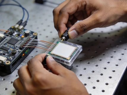
One of the main technical goals is to create optical connectivity that can handle data transfer rates up to 1.6 terabits per second (Tbit/s). This number, taken from company statements, reflects the bandwidth needed as AI models and datasets grow. Qualcomm's work in serializer-deserializer (SerDes) and optical digital signal processing (DSP) will be key, with the aim of reducing latency and increasing throughput between thousands of processors. High-throughput optical links are also a focus at CERN, where moving data at scale is a major challenge.
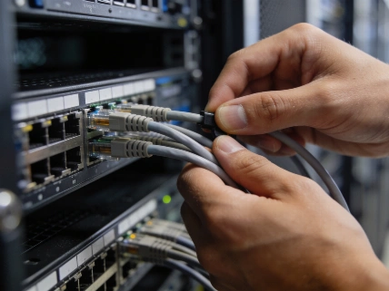
Modern AI data centers rely on large, tightly connected networks of accelerators, memory, and storage. As AI workloads grow, moving data efficiently between compute nodes becomes a limiting factor. The focus on optical interconnects shows that traditional copper-based networking is reaching its limits for speed and energy efficiency at this scale.
Financially, the deal gives Amazon warrants to buy 25 million shares of Qualcomm at $161.26 per share, a package worth about $4 billion if fully exercised. These warrants are linked to Amazon's commitment to purchase up to $60 billion in Qualcomm hardware over the next decade, with vesting in tranches through September 2036 and some already vested. This long-term structure is common in the semiconductor industry, where multi-year roadmaps are needed for research, development, and supply chain planning.
Qualcomm also plans to expand its use of AWS AI infrastructure, including Amazon Bedrock, for electronic design automation (EDA) workloads. The goal is to shorten chip design cycles, though no specific numbers or timelines have been shared. This creates a feedback loop: Qualcomm will use Amazon's AI tools to speed up its own chip development, while Amazon benefits from the resulting hardware advances.
Amazon has a history of developing custom silicon for AWS, such as Graviton and Inferentia chips. Adding Qualcomm's semiconductor expertise could lead to more specialized chips optimized for AI inference, rather than general-purpose cloud computing. The companies have not shared details on manufacturing partners, deployment schedules, or the specific AI workloads the new silicon will target.
For now, the collaboration is at the announcement stage. As of mid-September 2026, there are no independent benchmarks, deployment figures, or third-party evaluations, and no reports of regulatory approval or changes to the deal. The companies present the partnership as a response to the rapid growth in AI compute, storage, and networking needs, but the real impact will depend on execution and measurable performance improvements.
Thermal management and energy efficiency remain ongoing challenges for AI data centers, as seen in recent coverage of liquid cooling solutions. The Qualcomm-Amazon partnership's focus on power-efficient compute and high-bandwidth optical links suggests they are aware of these issues, though they have not provided specific energy-use targets or cooling plans. Research from the Max Planck Society and Harvard has highlighted the need for energy-efficient architectures in future AI infrastructure.
This collaboration points to a trend toward more integrated hardware and software stacks, with hyperscale operators and chipmakers working together to meet the demands of large-scale machine learning. Without independently verified results or deployment timelines, the announcement is best seen as a strategic alignment rather than a proven technical advance. The real test will come when these custom silicon and optical solutions are deployed at scale and put to work in real AI workloads.
AI inference is the process of running trained machine learning models on new data to generate predictions or classifications. In large data centers, inference workloads can involve thousands of processors exchanging large amounts of information in real time. Optical connectivity, such as fiber-optic links, offers higher bandwidth and lower latency than copper connections, making it increasingly important for scaling AI systems. Custom silicon refers to chips designed for specific tasks, like accelerating AI inference, rather than general-purpose computing. Bringing these technologies together is central to the ongoing development of AI infrastructure.